Using the Virtex-6 Embedded Tri-Mode Ethernet MAC Wrapper v1.4 with the ML605 Board
Whenever I get a new Xilinx development board I go through the tedious process of porting my circuits that use Ethernet communication to the new board. To save other people the pain I went through to get this to work I have written this blog which outlines the changes you need to make to the automatically generated Ethernet MAC wrapper to make the default echo circuit work. Note that these instructions only apply to the Xilinx ML605 development board:
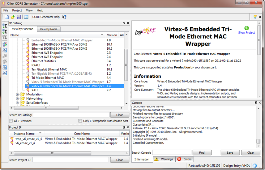
I have tested these instructions with ISE version 12.4 (running on Windows 7 64-bit). Step 1: generate the wrapper from Core Generator:
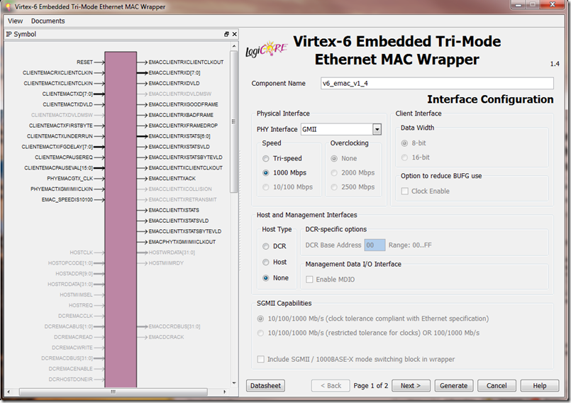
Select the GMII interface and leave the other options unchanged:
Make sure that you have jumpers J66 and J67 over pins 1 and 2 for GMII operation. (You can try to get SGMII working by setting the jumpers overs pins 2 and 3. Good luck.)
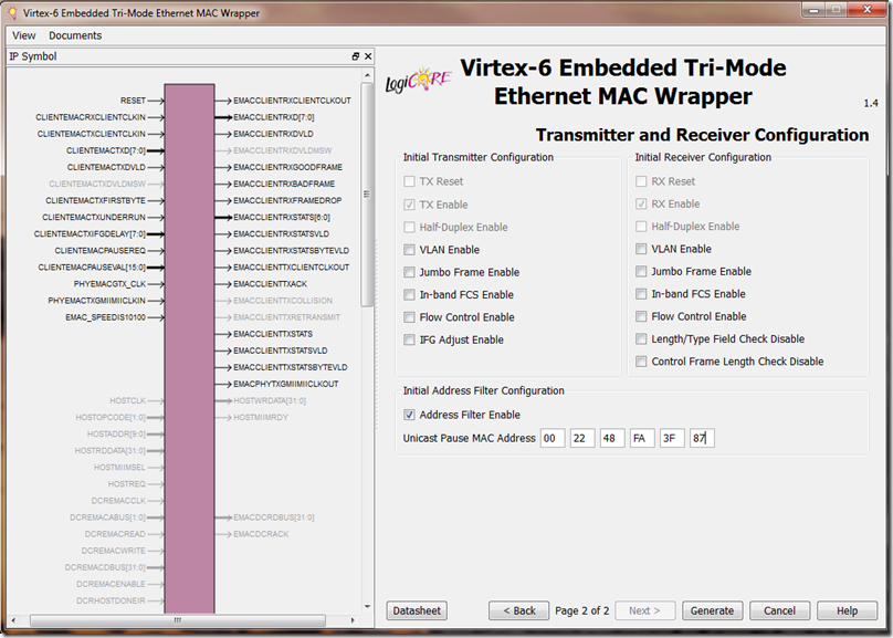
On the next screen I suggest you set the address filter feature (please don't steal the address below especially if you work at Microsoft).
Now generate the core. Now you need to edit the UCF file. You should read the user guides for the Ethernet MAC and the wrapper to work out the details for your particular situation but here are some of the things you will need to do. First, add the necessary pin assignments. For reset I use the centre push-button:
NET "RESET" LOC = G26; # Centre push-button
For clocking I use the differential 200MHz clock inputs from the Epson crystal from which I will derive the 125MHz clock to drive the Ethernet sub-system:
 INST SYSCLK_N LOC = H9 ;
INST SYSCLK_P LOC = J9 ;
NET SYSCLK_P TNM_NET = sysclk;
TIMEGRP sysclk_grp = sysclk;
TIMESPEC TS_sysclk = PERIOD sysclk_grp 5 ns HIGH 50 %;
I like to reset the PHY chip while the clocking circuitry is waiting to start up:
NET "PHY_RESET" LOC = "AH13";
You will need to wire up the GMII interface pins:
 INST "GMII_TXD<0>" LOC = "AM11";
INST "GMII_TXD<1>" LOC = "AL11";
INST "GMII_TXD<2>" LOC = "AG10";
INST "GMII_TXD<3>" LOC = "AG11";
INST "GMII_TXD<4>" LOC = "AL10";
INST "GMII_TXD<5>" LOC = "AM10";
INST "GMII_TXD<6>" LOC = "AE11";
INST "GMII_TXD<7>" LOC = "AF11";
INST "GMII_TX_EN"  LOC = "AJ10";
INST "GMII_TX_ER"  LOC = "AH10";
INST "GMII_TX_CLK" LOC = "AH12";
INST "GMII_RXD<0>" LOC = "AN13";
INST "GMII_RXD<1>" LOC = "AF14";
INST "GMII_RXD<2>" LOC = "AE14";
INST "GMII_RXD<3>" LOC = "AN12";
INST "GMII_RXD<4>" LOC = "AM12";
INST "GMII_RXD<5>" LOC = "AD11";
INST "GMII_RXD<6>" LOC = "AC12";
INST "GMII_RXD<7>" LOC = "AC13";
INST "GMII_RX_DV"  LOC = "AM13";
INST "GMII_RX_ER"  LOC = "AG12";
INST "GMII_RX_CLK" LOC = "AP11";

and you will need to comment out some constraints and also remove the GTX_CLK reference because we are going to derive this from the 200MHz clock.
In the top level design file you will need to make several changes including adding ports for the 200MHz clock input and the PHY reset and remove the GTX_CLK:
      -- Reference clock for IODELAYs
     -- REFCLK                   : in  std_logic;
        SYSCLK_N, SYSCLK_P : in std_logic ;

        PHY_RESET : out std_logic ;
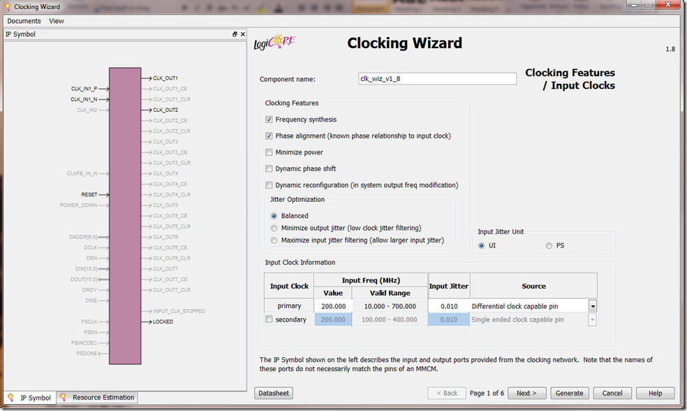
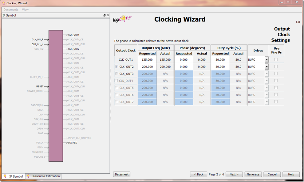
To generate the clocks you should run the Clock Wizard and specify a 200MHz source clock with differential inputs:
On the next screen define a 125MHz clock output and a 200MHz clock output. Either select BUFG outputs (and then comment out the manually instantiated buffers in the top level design and replace them with regular signal assignments) or select no output buffer and make use of the IBUFGs and BUFGs in the existing design.
Wire up the clock generation core in the top level module:
   clk_wiz : clk_wiz_v1_8
  port map
   (-- Clock in ports
    CLK_IN1_P => SYSCLK_P,
    CLK_IN1_N => SYSCLK_N,
    -- Clock out ports
    CLK_OUT1           => GTX_CLK,
    CLK_OUT2           => REFCLK,
    -- Status and control signals
    RESET              => reset_i,
    LOCKED             => locked);
I used the locked output to control the PHY reset.
Now you should be able to generate the bit-stream and test it out. You can add a ChipScope probe to see what is going on:
 icon : chipscope_icon port map (CONTROL0 => CONTROL);

ila : chipscope_ila port map (CONTROL => CONTROL,
                              CLK => ll_clk_i,
                              DATA => DATA,
                              TRIG0 => TRIG0);

trig0(0) <= rx_ll_sof_n_i ;
DATA(7 downto 0) <= rx_ll_data_i ;
DATA(8)  <= rx_ll_sof_n_i ;
DATA(9)  <= rx_ll_eof_n_i ;
DATA(10) <= rx_ll_src_rdy_n_i ;
DATA(11) <= rx_ll_dst_rdy_n_i ;
DATA(19 downto 12) <= tx_ll_data_i ;
DATA(20) <= tx_ll_sof_n_i ;
DATA(21) <= tx_ll_eof_n_i ;
DATA(22) <= tx_ll_src_rdy_n_i ;
DATA(23) <= tx_ll_dst_rdy_n_i ;
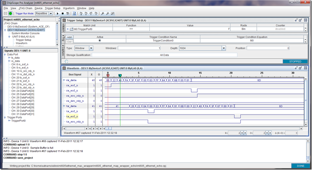
and you should be able to observe an address-swap Ethernet echo:
which is also confirmed in WireShark:
Now, how do you send a raw Ethernet packet from a Windows 7 64-bit machine? That might be the subject of another blog post.
Good luck!
Satnam
