Compiling C# Programs into FPGA Circuits: Factorial Example
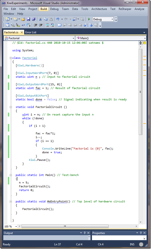
This blog article gives a practical introduction to how C# programs can be compiled into FPGA circuits using the Kiwi system developed by myself and David Greaves at the University of Cambridge Computer Lab. Our starting point will be a C# program developed inside Visual Studio 2010 for computing factorial:
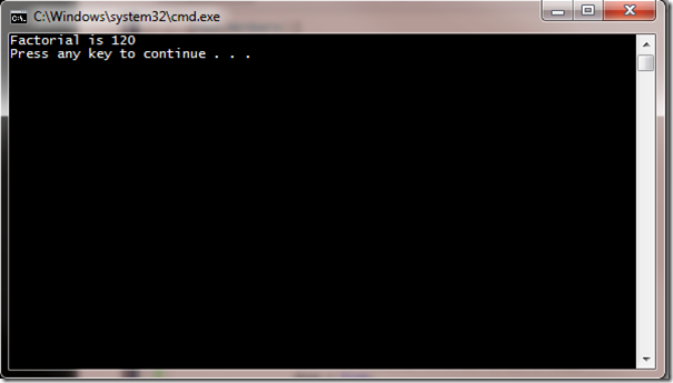
This program can be compiled and executed inside Visual Studio to report the factorial of 5 (i.e. 120).
However, using our Kiwi system this program can also be converted into a Verilog circuit. The program is decorated with some custom attributes which specify which static method should be turned into hardware; the number of bits used to represent input and output ports and how the circuit should behave relative to a circuit clock.
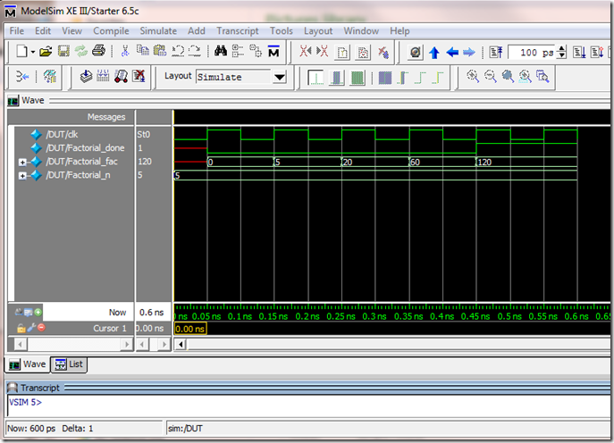
The generated Verilog netlist can be simulated using a Verilog simulator. The Modelsim simulator output produced by simulating this circuit with an input of 5 for the factorial circuit is shown below. After a few clock cycles the result 120 is produced and the done output bit goes high.
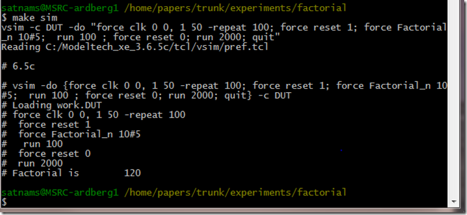
Or if you like you can run the simulation on the command line:
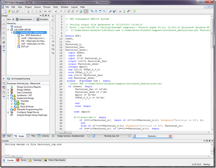
The generated Verilog can be used as input to the Xilinx design tools to generate a programming bit-stream to program an FPGA. The screen-shot below also includes a top-level module which instantiates some debugging input and sets the default input to the factorial circuit to be 5.
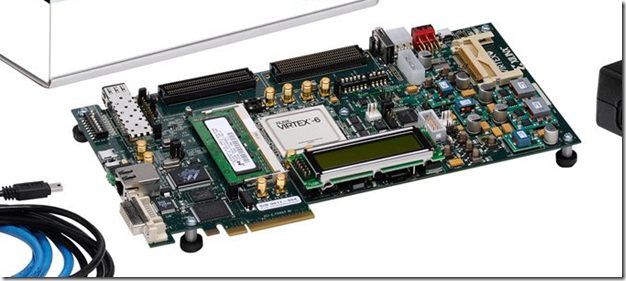
The generated programming bit-stream can then be run on a real FPGA board. I used a Xilinx ML605 which has a Xilinx Virtex-6 XC6VLX240T-1FG1156 FPGA on it:
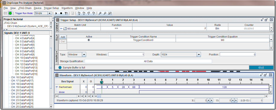
I can check the functionality of the circuit by running a software logic analyzer on my PC which reports the value of internal signals of the circuit running on the FPGA.
The logic analyzer shows that this circuit indeed computes the factorial of 5 to be 120 after 4 clock cycles. This circuit is running at 100MHz.
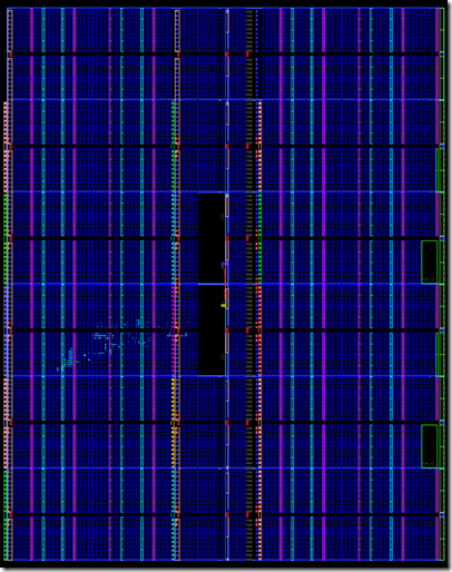
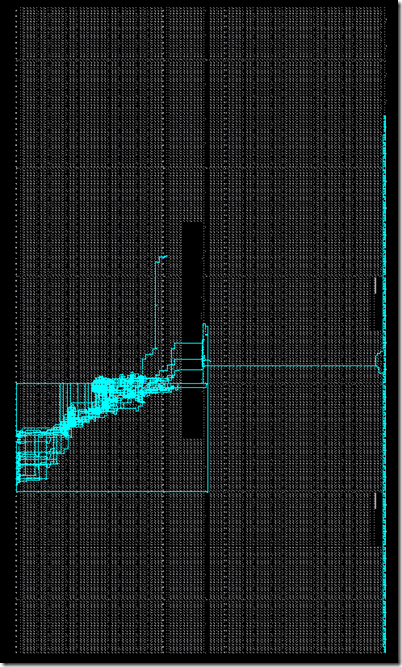
You can get a warm and fuzzy feeling by looking at the floor-plan of the generated circuit (light blue specks on the middle left hand side) which also includes the debug circuitry required to support the logic analyzer:
This lower-level view shows the actual routing tracks for the wires.
